
To fulfill the Center's mission, the Center’s research framework shown below focuses on two Thrusts that encompass four Science and Technology Development Areas (STA). Six discrete projects comprise these four STAs.
The goal is to integrate research and development in “end-to-end”, molecules-to-systems approach.
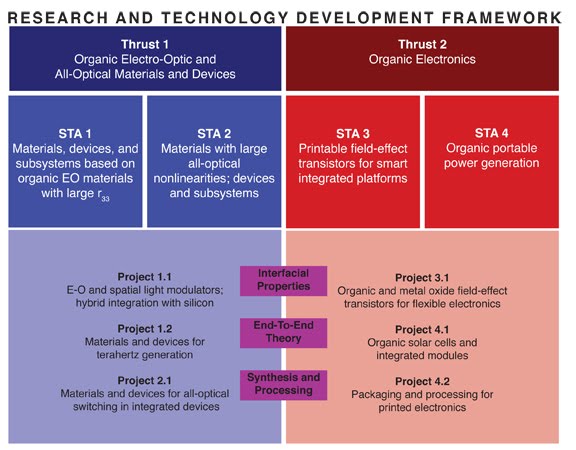
Thrust 1 Overview
The vision of this thrust is to develop "transformative" electro-optic (EO) and all-optical (AO) materials and devices for light-weight, low power, and ultrahigh-speed information processing. This will be achieved through "end-to-end" cross-disciplinary collaboration in theory, materials synthesis, processing and device design and fabrication. The X2 and X3 activity of materials will be significantly enhanced through improved NLO chromophores and materials that are developed through theory-guided structural design, innovative synthetic chemistry and self-assembly.
The research within Thrust 1 is organized into two major science and technology areas, one on light-emitting devices and their integration with organic-field-effect transistors, and another on flexible portable photovoltaic cells combined with packaging and patterning technologies:
STA 1
Materials, Devices, and Subsystems Based on Organic EO Materials with Large r33
STA 1 is organized into two main research projects:
- Project 1.1: E-O and spatial light modulators; hybrid integration with silicon
- Project 1.2: Materials and devices for terahertz generation
STA 1 is focused on the molecular engineering of materials with ultrahigh electro-optic
activities and suitable optical attenuation, thermal stability, and photochemical stability,
and which can be incorporated into novel device structures for applications in ultralow
voltage EO modulators, silicon-based photonics, and terahertz emitters and sensors.
STA 2
Materials with Large All-Optical Nonlinearities, Devices and Subsystems
STA 2 is organized into two main research projects:
- Project 2.1. Materials and devices for all-optical switching in integrated devices
STA 2 is focused on the development of materials with very large χ3 properties that can
be used for all-optical switching and free-space signal processing.
Thrust 2 Research Projects
Project 3.1
Organic and Metal Oxide Field-Effect Transistors for Flexible Electronics
Lead: Denise Wilson
This project is focused on developing organic semiconductors with thin-film hole and electron mobilities >10 cm2/Vs, (i.e., greater than that of amorphous silicon). CMDITR will develop surface-modifying agents that will help with this issue, as well as improved adhesion at organic/organic and inorganic/organic interfaces. CMDITR will also develop new dielectric materials that can be coated into thin (< 200 nm) films with high dielectric strength (> 2 MV/cm), low leakage current (< 1 μA/cm2), and high capacitance density (> 50 nF/cm2).
- Electron-vibration coupling in organic semiconductors.
- Interface between an organic semiconductor and a gold electrode
- Impact of packing density of a self-assembled monolayer (SAM) on surface modifications
- Organic field-effect transistors with selectively doped contacts
- Hybrid complementary inverters on flexible substrates with high gain
- Improved Performance and Stability of OFETs
- Modeling of OFETs
Project 4.1
Organic Solar Cells and Integrated Modules
Lead: Neal Armstrong
The goal of our research on organic solar cells is to advance the understanding of the physics that governs their operation and to develop models that can be used to guide the optimization of their performance. Our objective will be to increase the efficiency of devices based on bulk heterojunctions and multilayer geometries (> 10% on glass substrates and > 7% on light-weight flexible substrates) by the synthesis of new molecules and polymers with optimized properties. Other important aspects of our activities include the development of new transparent conducting layers intended as replacements for ITO.
- Exciton dissociation and charge-recombination processes in pentacene-C60 solar cells
- Controlled Polymerization of P3HT for OPV Devices
- Polymer solar cells with an inverted structure using an ultrathin Al2O3 buffer layer
- Enhanced Photovoltaic Efficiency of Polymer/Fullerene Bulk Heterojunction Solar Cells by Nanostructure Engineering
- Novel Configurations for Efficient OPV Modules
- Low Temperature Gas Phase Processing of Oxides
- Polymer thermogalvanic cells for solar thermal and waste heat harvesting
- Exploration of semiconductor nanoparticles as diffraction grating elements and light emitters
- Scanning Probe Methods For Characterizing Charge Transport in Photodiodes
Project 4.2
Packaging and Processing for Printed Electronics
Lead: Bernard Kippelen
A critical objective of this project will be to develop thin film encapsulation layers with permeation rates at or below 10-5 g/m2/day and to integrate them with organic photovoltaic cells, OLEDs, and organic circuits. Additional efforts to reduce the number of layers and processing steps needed for the encapsulation will be performed with the goal of a single or bilayer encapsulation film.
- Critical Levels of Water Vapor Transport for Shelf Lifetime in OPVs
- Improving the Flexibility of Barrier Coatings
- Conducting AFM Probes of Carbon Nanotube Transparent Electrodes
- The Integration of OPV and OLED Devices Into a Single Platform
- Nanoimprinting-based texturing of solar cell materials
- Thermochemical nanolithography (TCNL) Patterning